> For the complete documentation index, see [llms.txt](https://soups-misc.gitbook.io/fpga-training/llms.txt). Markdown versions of documentation pages are available by appending `.md` to page URLs; this page is available as [Markdown](https://soups-misc.gitbook.io/fpga-training/fpga-kai-fa-liu-cheng-yu-gai-nian.md).
# FPGA開發流程與概念
## 名詞與概念簡介
* FPGA如其名,主要由邏輯閘(GATE)構成
* FPGA開發主要透過Verilog/VHDL,也就是HDL開發(HDL Hardware Description Language又稱為硬體描述語言)
* 一般的程式主要是將程式碼編譯後產生執行檔,交由CPU執行執行檔
* HDL則會產出數位邏輯電路,並在FPGA板上完成邏輯閘接線.
* 另一個常見名詞RTL為register-transfer level,意同HDL.
## 設計流程
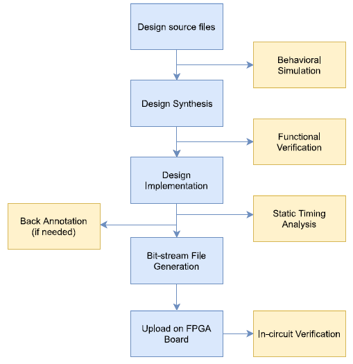
整體的FPGA設計流程圖如下概括,並以詳述各項細節,下面一些開發流程也會圍繞著相同概念說明各項細節
FPGA Desgin flow
## 1. Design source file
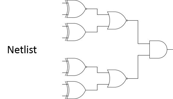
當設定好要開發的功能細節之後,首先第一步就是先撰寫HDL source code.以下為一個簡單的HDL 加法器範例:
```verilog
module Full_Adder( A, B, Cin, Sum, Cout );
input A, B, Cin;
output Sum, Cout;
wire W1, W2, W3;
xor xor1( W1, A, B );
and and1( W2, W1, Cin );
and and2( W3, A, B );
xor xor2( Sum, W1, Cin );
or or1( Cout, W2, W3 );
endmodule
```
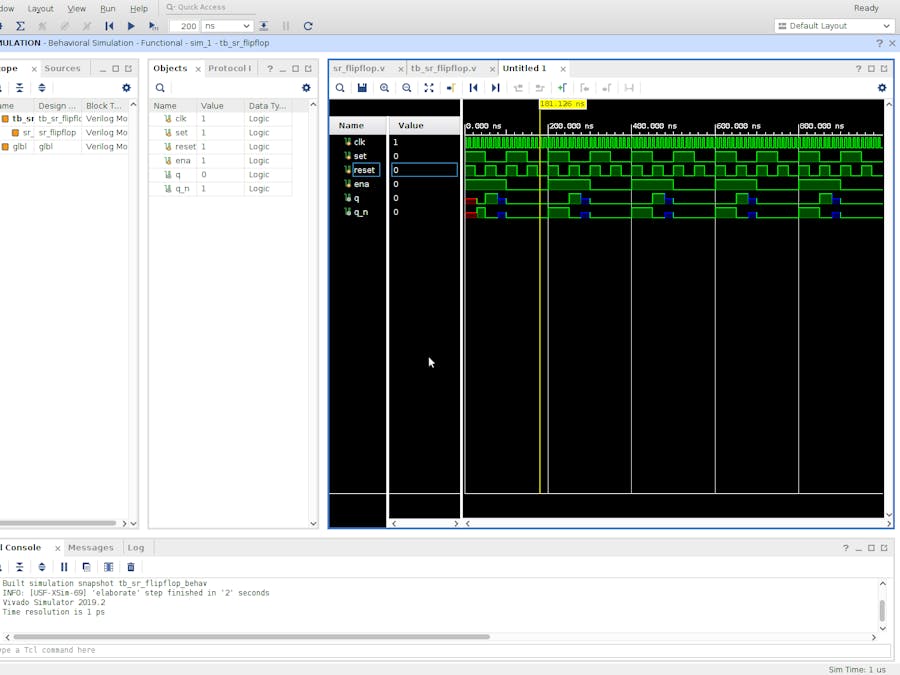
## 2. Behavioral Simulation
寫完HDL之後通常會寫testbench觀察波形、驗證行為正確性.